Thermal Materials Tailored to Your Package and Process Requirements
We provide TIM1 material selection and custom development for thermal transfer between the die and package lid. Material designs are adjusted according to bond line thickness, thermal performance, interface properties, and assembly conditions to balance heat dissipation efficiency with long-term reliability.
Establishing an Effective Thermal Interface from the Die
TIM1 is located between the die and lid in a lidded package, while TIM1.5 is used in lidless packages to directly connect the bare die to a heat sink or cold plate. Both fill gaps between mating surfaces, reduce thermal contact resistance, and help transfer heat away from the die.
TIM1 | Thermal Interface Inside the Package
TIM1 connects the back of the die to the package lid and must provide a thin bond line, complete coverage, and stable contact despite package deformation.
TIM1.5 | Thermal Interface Between the Bare Die and Cooling Structure
Used in lidless packages to directly connect the bare die to a heat sink or cold plate, TIM1.5 must balance low thermal resistance, interface conformity, and the assembly stress applied to the die.
TIM2 | Thermal Interface Between the Package and Cooling Structure
TIM2 is located between the package lid and heat sink or cold plate, helping transfer heat from the package to the external cooling system.
Applications
AI accelerators
Server Processors
HPC Computing Chips
Multi-Die Lidded Packages
Thermal Management and Reliability Challenges
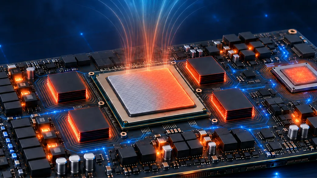
High-Power, Large Packages Place Greater Demands on Thermal Interfaces
As chip power consumption and package size increase, TIM1, TIM1.5 must not only reduce initial thermal resistance but also withstand temperature changes and package deformation. The material, bonded interfaces, and assembly process must work together to maintain long-term thermal performance.
01
Challenge
High Heat Density and Interface Thermal Resistance
Concentrated hot spots increase the cooling load, while material thermal conductivity, bond line thickness, and contact quality on both sides affect heat transfer efficiency from the die to the lid.
02
Challenge
Thin Bond Lines and Complete Coverage
A thin-layer design helps reduce bulk material thermal resistance, while gap filling and coverage must be controlled to prevent voids or locally unfilled areas.
03
Challenge
Package Warpage and Thermal Stress
Differences in thermal expansion among the die, lid, and substrate subject the interface to shear, tensile stress, and gap changes as temperatures fluctuate, placing demands on material compliance and adhesion stability.
04
Challenge
Material Pump-Out and Interface Degradation
Repeated thermal cycling may cause pump-out, dry-out, or delamination, degrading contact quality and increasing thermal resistance and the risk of localized hot spots.
TIM1, TIM1.5 Materials Developed to Your Specifications
Different package designs have different requirements for thermal performance, bond line thickness, mechanical properties, and process compatibility. LiPOLY adjusts material formulations and properties according to application specifications to support sampling, process evaluation, and package validation.
vertical_align_center
Thermal Performance and Bond Line Thickness
Define the material’s thermal performance and target bond line thickness based on power consumption, target thermal resistance, and bond gap, balancing a thin-layer design with effective gap filling.
Inputs
target thermal resistance, thermal conductivity, BLT, and bonding area.
massage
Conformability and Mechanical Properties
Adjust material compliance, adhesion, and deformability according to die size, bonding-surface materials, and package deformation conditions.
Inputs
hardness or modulus, adhesion requirements, warpage range, and rework requirements.
tile_medium
Application and Assembly Processes
Adjust flow and handling properties according to the material application method, assembly sequence, and production-line conditions; curing conditions for curable materials can also be defined as required.
Inputs
application method, viscosity, working life, assembly pressure, curing temperature, and curing time.
solar_power
Operating Environment and Reliability
Define material evaluation and validation conditions based on operating temperature, load variations, and reliability requirements to assess thermal resistance and interface performance over long-term use.
Inputs
Information you can provide: operating temperature, thermal cycling, power cycling, temperature-humidity conditions, and acceptance criteria.
From Specifications to Application Validation
01
Requirements Review
Review the package structure, target specifications, and process limitations.
02
Material Development and Sampling
Select materials or adjust formulations according to the requirements and provide samples.
03
Process and Package Testing
Verify bond quality and thermal performance under the customer’s application and assembly conditions.
04
Specification Confirmation and Implementation
Adjust the material based on test results and confirm the product specifications and subsequent implementation conditions.
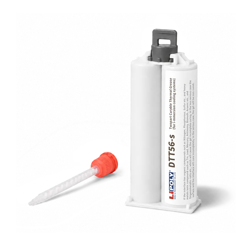
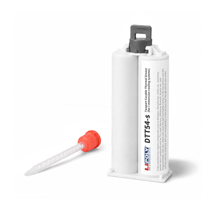
Provides thin-layer gap filling and curable forming properties and can be evaluated according to bonding conditions and process requirements.
Bond Line Thickness: 10 μm
Cured Hardness: 40 Shore A
Curable design that reduces the risk of material displacement
The values above are typical catalog values and are not guaranteed specifications; actual thermal resistance, process conditions, and reliability performance must be confirmed based on the package structure and test results.
Have Different Specification Requirements?
If your required bond line thickness, thermal performance, or process conditions differ from our existing products, submit your target specifications to discuss a custom development solution.
Power density inside AI GPU modules keeps climbing, pushing the GPU, HBM, and VRM ever closer to their thermal design limits. This article focuses on GPU chip-level TIM, examining how PCM900 phase change material works and the reliability data behind it.
Package warpage and component height variation can raise HBM junction temperature and trigger thermal throttling. This article explains how gap filler materials address this challenge and reviews Ultra3065's specifications and reliability data.
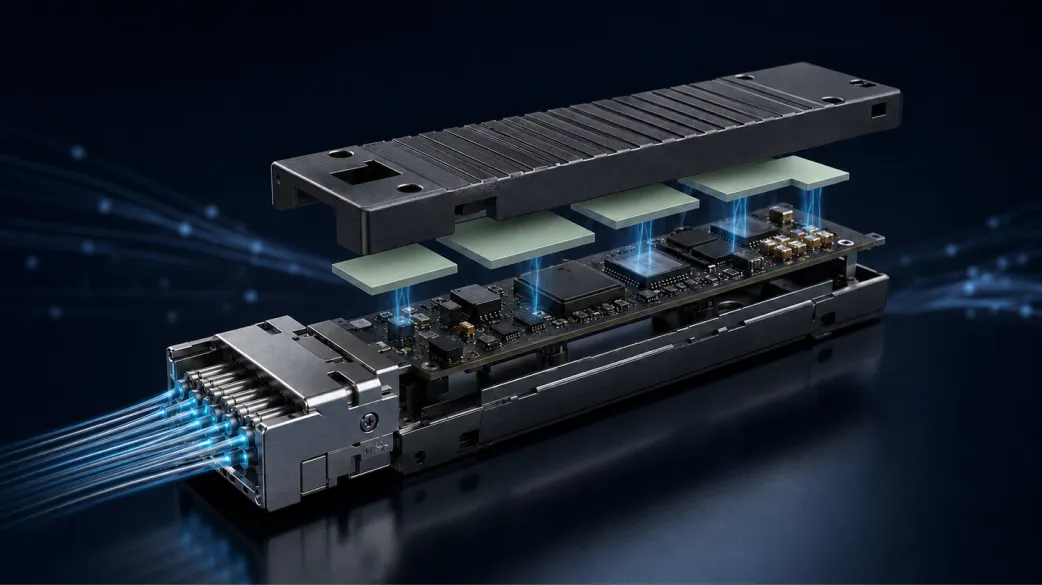
Optical module power is rising fast — TIM selection must now balance thermal performance with optical surface cleanliness. This article explains the siloxane contamination mechanism and offers non-silicone pad/putty selection guidance.
Submit Your Package Conditions to Discuss a Custom TIM1,TIM1.5 Solution
In the “Requirements” field, provide the application conditions you have confirmed so our technical team can recommend suitable materials and development options.
support_agent
Technical Support
Evaluate the best thermal solution
trackpad_input
Material Selection
Quickly identify the right material combination
dashboard_2_edit
Custom Solutions
Create dedicated material solutions according to your needs
Package and Bonding: Die dimensions, bonding-surface materials, and target thickness (BLT).
Thermal Performance: Operating temperature, target thermal resistance, or thermal conductivity.
Assembly Process: Application method, assembly pressure, and curing conditions.
Reliability: : Test conditions, acceptance requirements, or issues to be improved in the current material.
You may begin by providing the information already available; our technical team will work with you to confirm the remaining details.
Thermal Solutions Expert
SHIU LI TECHNOLOGY CO., LTD.
Taoyuan City, Bade District, Yongfeng Road, No. 435