



Height Variation and Large Gaps — An Often-Overlooked Variable in Advanced Packaging Thermal Design
In the advanced packaging used in AI GPU modules (such as 2.5D/3D heterogeneous integration), height differences frequently arise between the GPU logic die, surrounding HBM stacks, and the package lid due to process and assembly tolerances. Academic literature indicates that variations in lid flatness, package warpage, and surface topography cause non-uniform TIM bond-line thickness and contact pressure distribution, further increasing interface thermal resistance and the temperature gradient within the module. Other research further explains that, in addition to the stress caused by CTE (coefficient of thermal expansion) mismatch between dies in large 2.5D assemblies, the self-weight of stacked dies, heat spreader lids, and copper conduction layers can also cause non-uniform bending and warpage of the interposer — with HBM modules being one of the components contributing to this load. Field engineering experience also indicates that when PCB warpage, lid co-planarity, and component height variation stack together, the cumulative deviation on a densely populated board can exceed 0.3 mm — not a small tolerance when considering the dozens of thermal contact points on a single board.
Against this backdrop, warpage control and thermal management in advanced packaging have been identified by relevant IEEE research as one of the key issues affecting manufacturing yield and long-term reliability, and is an interface scenario that must be identified first when selecting TIM materials.
What Are the Potential Consequences of Unaddressed Height Variation and Gap Issues?
Insufficient gap filling due to height variation most directly results in elevated interface thermal resistance, which in turn raises die junction temperature. Taking HBM as an example, engineering guidelines indicate that a single HBM3E-class memory stack can generate over 20 watts of thermal load, typically requiring a TIM with thermal conductivity greater than 5 W/m·K to keep junction temperature within the safe range below 85°C; exceeding this threshold may trigger thermal throttling, signal degradation, and long-term reliability risk. Academic review research has also provided concrete data: after introducing a thermal management package (TMP) to improve thermal coupling between GPU and HBM, HBM junction temperature can be reduced by approximately 10.3°C, with signal jitter also decreasing by roughly 4.54% — demonstrating a direct link between thermal design and signal integrity, not merely a temperature number. At the system level, industry observations also note that uneven cooling in data centers can create localized hot spots and airflow recirculation, potentially triggering throttling or even compute job interruption — real operational costs.
How Gap Filler Materials Address This Challenge
Gap filler materials are a category of TIM specifically designed for large-gap and height-variation scenarios. Unlike higher-hardness thermal pads, gap fillers typically offer greater compressibility, allowing them to deform under assembly pressure to conform to component surfaces at different heights, avoiding unfilled voids that can result from materials that are too rigid. Industry data shows that, compared with a simple air gap, introducing a gap filler can reduce interface thermal resistance by approximately 80% to 95%; thermal conductivity varies significantly depending on the base resin and filler design, with typical silicone-based gap fillers falling in the 1–8 W/m·K range, while advanced ceramic-filled formulations can reach 20 W/m·K or higher. Academic research also notes that gap fillers used between high-power components and heat sinks must balance thermal conductivity with electrical insulation performance, which is why filler design in this material category requires a trade-off between thermal conductivity and insulation.
In terms of material design principles, TIM interface thermal resistance can be approximately expressed by the simplified formula: R ≈ BLT ÷ k (where R is thermal resistance per unit area, BLT is bond-line thickness, and k is thermal conductivity). This relationship shows that, to maintain a similar thermal resistance target, thermal conductivity must increase roughly proportionally as bond-line thickness increases. As an illustrative example: suppose a chip-level TIM at a 50-micron (0.05 mm) bond-line thickness achieves a certain thermal resistance level with a thermal conductivity of 5 W/m·K; if the interface gap is enlarged fivefold to 250 microns (0.25 mm), maintaining a similar thermal resistance level would require thermal conductivity to likewise increase roughly fivefold, to approximately 25 W/m·K. This illustrates why gap filler materials, as a category, typically require thermal conductivity specifications an order of magnitude higher than chip-level TIM-1 materials — a physical consequence of the enlarged interface geometry, not a specifications contest.
(Note: the above is a simplified, illustrative calculation intended only to demonstrate the proportional relationship between BLT and thermal conductivity. The values are hypothetical and used for ease of understanding; they are not measured BLT or thermal resistance data for any specific product. Actual total TIM thermal resistance also includes contact resistance at both interfaces and is not determined solely by the simplified formula above; actual performance should be based on the manufacturer's published thermal resistance/impedance test data.)
Ultra3065 Technical Specification Analysis
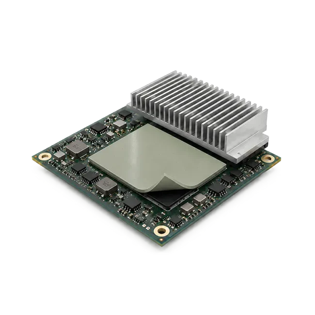
LiPOLY Ultra3065 is an ultra-high thermal conductivity thermal interface material in the gap filler category, with a thermal conductivity of 30.0 W/m·K — placing it at the high end of thermal performance for gap filler materials relative to the 5 W/m·K threshold suggested by the engineering guidelines cited above and the 1–8 W/m·K range typical of silicone-based materials. The material is designed with Shore OOO 65 hardness, balancing compressible conformability with the mechanical support needed during assembly, allowing it to compensate for component height variation and surface unevenness. In terms of electrical performance, Ultra3065 has a dielectric breakdown strength of 9 KV/mm, providing the insulation safety margin required for high-power applications. The product is available in customizable thickness and dimensions for specific gap requirements. Typical applications include high-power scenarios such as AI servers, GPU modules, AI accelerators, CPUs, HBM packages, and power modules, as well as data center servers, networking, and telecom equipment.
| Property | Specification |
|---|---|
| Product Model | Ultra3065 |
| Thermal conductivity | 30.0 W/m·K |
| Hardness | Shore OOO 65 |
| Dielectric Breakdown Strength | 9 KV/mm |
Note: The data above are typical values obtained by LiPOLY using its internal TIM Tester method and the ASTM D5470 test method, provided for design reference only and not as guaranteed product specifications. Actual performance should be pre-verified under the applicable application conditions.
Reliability Test Results
Ultra3065 has undergone the following four reliability tests, all with a "Pass" result:
| Test Item | Test Condition | Test Result |
|---|---|---|
| High-Temperature Aging | 125°C, 1,000 hours | Pass |
| High-Temperature / High-Humidity (HAST) | 85°C / 85% RH, 1,000 hours | Pass |
| Thermal Cycling | -40°C ↔ 125°C, 500 cycles | Pass |
| Low-Temperature Test | -60°C, 1,000 hours | Pass |
It should be noted that the currently available datasheet provides only "Pass/Fail" results for the above four tests and does not publish quantitative pre- and post-test thermal resistance values, as is available for some other products. For more complete engineering specification data for design evaluation, please contact the LiPOLY technical team.
Conclusion
Unaddressed height variation and large gaps in advanced packaging can lead to HBM thermal throttling and signal degradation. This article explains how gap fillers work and reviews Ultra3065's specifications and reliability results.
FAQ
Q: What is the difference between gap filler materials and conventional thermal grease or thermal pads?
Gap filler materials typically offer higher compressibility than standard thermal pads, making them suitable for filling larger, uneven height variations. Compared with thermal grease, their solid or semi-solid form also reduces the risk of pump-out and material extrusion. Actual material selection should still be evaluated individually based on gap dimensions, tolerances, and assembly pressure conditions.
Q: Does a higher thermal conductivity always mean better thermal performance?
Not necessarily. Actual thermal performance depends on the material's total thermal resistance, which includes both the material's own bulk thermal resistance and the contact resistance at both interfaces. If the material cannot fully conform to the surfaces and air gaps remain, actual performance will be compromised even with a high thermal conductivity value — making compressibility and surface conformity equally important considerations in material selection.
References
- Lid flatness, warpage, and surface topography variations causing non-uniform TIM bond-line thickness and contact pressure: CAPLINQ, “2.5D Packaging | Advanced Packaging”
- Self-weight of dies, heat spreader lids, and stacked components (including HBM modules) in 2.5D assemblies causing non-uniform interposer bending and warpage: arXiv, “STAMP-2.5D: Structural and Thermal Aware Methodology for Placement in 2.5D Integration”
- Warpage control and thermal management in 2.5D packaging as a key factor in manufacturing yield and reliability: IEEE Xplore, “Design Guideline of 2.5D Package with Emphasis on Warpage Control and Thermal Management”
- Practical engineering discussion of cumulative tolerance from PCB warpage, lid co-planarity, and component height variation: 3G Shielding, “Thermal Gap Pad Guide: Specs, Compression & Failure Modes”
- Thermal resistance reduction from introducing gap filler materials and typical thermal conductivity range comparison: Modus Advanced, “Thermal Gap Pad Compression: Optimizing Performance Through Proper Selection and Application”
- Background on gap filler materials needing to balance high thermal conductivity with electrical insulation performance: PMC (NCBI), “A Comparative Study of Thermal Aging Effect on the Properties of Silicone-Based and Silicone-Free Thermal Gap Filler Materials”
- HBM3E single-stack thermal load exceeding 20 W, TIM thermal conductivity requirement (>5 W/m·K), 85°C junction temperature threshold, and thermal throttling risk: Wevolver, “HBM Memory: Complete Engineering Guide & Design Optimization 2025”
- Thermal management package (TMP) reducing GPU-HBM junction temperature by approximately 10.3°C and signal jitter by approximately 4.54%: MDPI, “Thermal Issues Related to Hybrid Bonding of 3D-Stacked High Bandwidth Memory: A Comprehensive Review”
- Uneven data center cooling causing localized hot spots, airflow recirculation, and operational costs from throttling/job interruption: Eziblank, “How Do AI Data Centres Manage Heat in High-Density GPU Clusters?”
- LiPOLY Ultra3065 Product Datasheet (Chinese / English / Japanese) — Internal Specifications
Related Products
NEW
Ultra High Thermal Conductive